What we're going to be doing today, is exploring the insides of the Zoom 505 II Multi-effects pedal. If you're interested in the history of this pedal, it can be found here (wikipedia entry) If you want one, they can be had on eBay for around $50, and around the same in your local used music equipment dealer's shop. Just a little bit about the unit before we start, it has 6 banks of 6 preprogrammed effects, for a total of 36 effects built in, that can be modified and saved using built in flash memory. It is powered by either 6VDC from 4 AA batteries, or 9VDC from an external power supply. On the back is the input jack, power supply jack, control in jack (more on that later) and output jack. Up top, you have the two footswitches, which are used to move between effects one by one, and if pressed simultaneously, activate the bypass and tuner. There's also the mod knob, which selects what part of the effect you are modifying, and finally the bank up/down switch, and a store switch right below it.

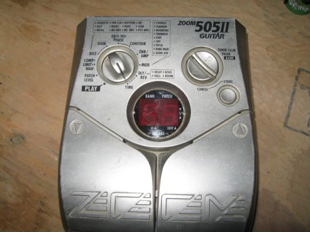
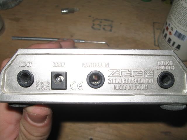
Time to tear it apart! One thing to make sure of, when you are messing with any electronic device, is make sure that it is not powered on, and if possible remove the power source. Although this device doesn't have any high voltage or dangerous components, it's still a good idea to remove power, so you don't fry anything while taking it apart.
The 505 II, like almost all guitar effects pedals, doesn't have an off switch, but is powered on when a cable is plugged into the input jack. Turn it over on it's back, and remove the 4 AA batteries if they are installed.
On the back, you'll immediately notice two screws right next to the battery door. Remove these, and look up near the top, right near the rear jack panel, you'll see two rubber pads. Pull these off, and remove the two screws that are below them. A good rule to go by when you are taking things apart, is to take pictures of where things go, and keep screws grouped together, either with a tray with compartments, or tape. In this case, all of the screws are the same, so it doesn't matter. Set them aside with the rubber pads.
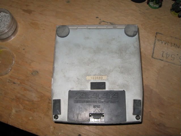
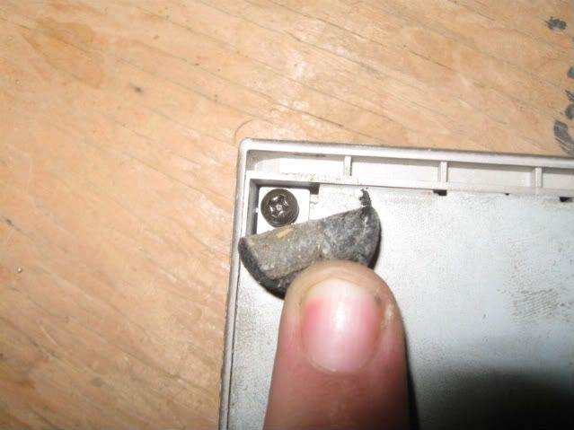
Lift up on the metal plate, you can either pick it up from the battery compartment, or use a screwdriver to pry up a corner near the top. Either way, it should come right off with no problems.
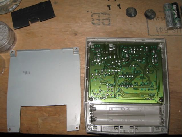
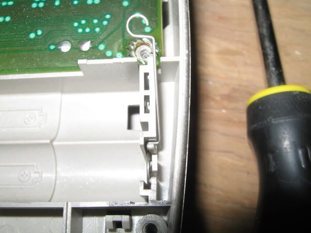
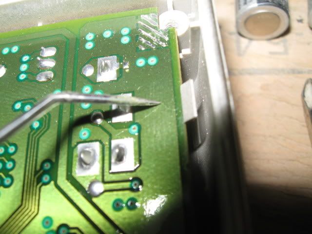
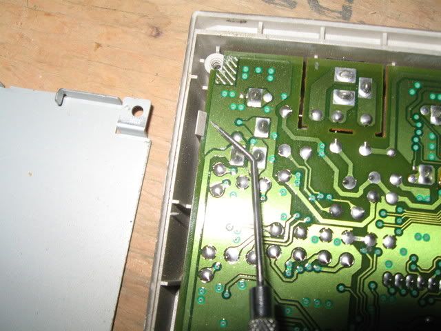
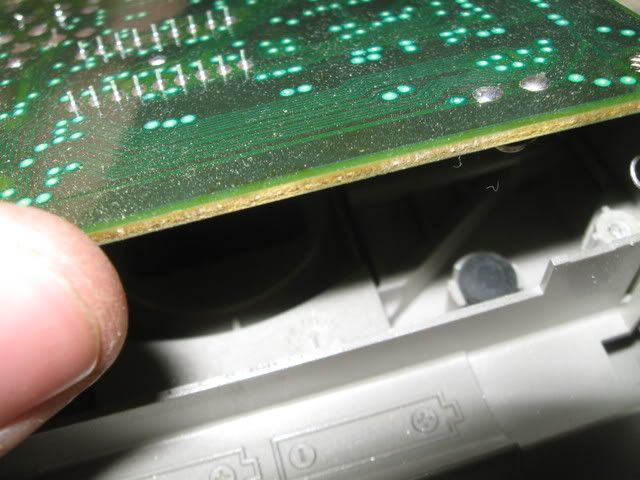
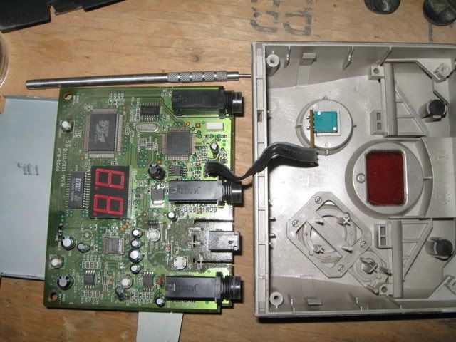
Now we get our first look inside. Notice the two screws right near the battery compartment. Remove these and set them aside. Now, right under the screws, the battery terminals meet the board. Pry these up and out of the way. Be careful not to let them pop out of the battery compartment, they can be a pain to get back in, speaking from experience here! Up near the top of the board, there are two tabs that are holding the board in. Push them aside, and pick up on the board from the bottom part, near the battery connectors, and pull it out. Since the jacks are attached to the board, and stick out a bit near the top, you'll have to pull out and down to remove the board. Be careful of the ribbon cable attached to the board as well, it's not very fragile, but still use caution when removing it.
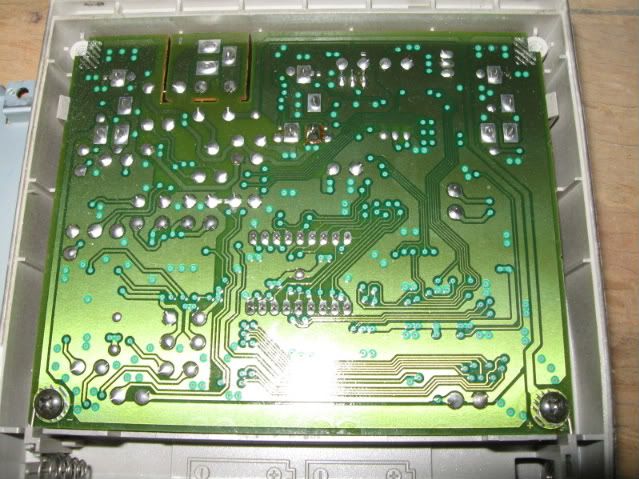
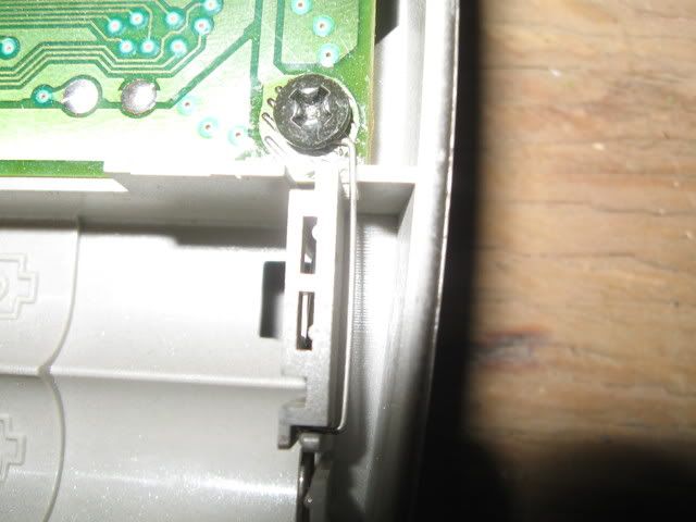
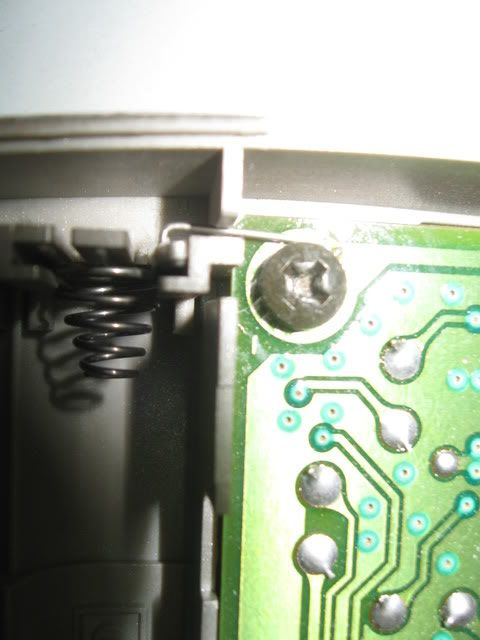
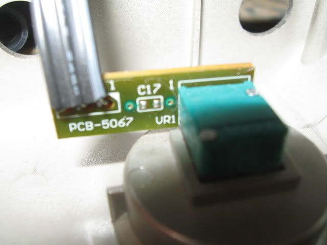
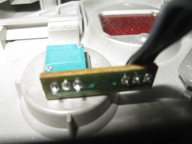
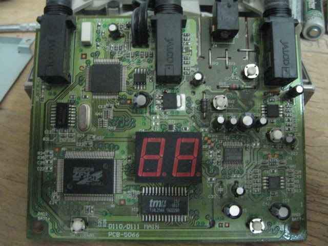
Lay the board on it's back, like shown in the picture. Now we can do some exploring, and see what makes this thing tick. First off, you'll notice that all of the buttons with the exception of the rotary switch, are just simple tactile switches. Also, the rotary switch just appears to be a potentiometer. Back to the main board, there are 10 ICs, along with two crystals, and a bunch of passive components.
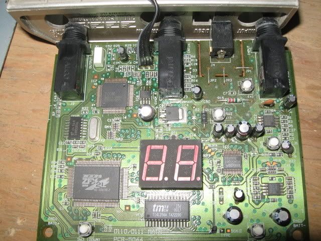
The first IC has the markings PCM3006T, which a search on Alldatasheet.com reveals that this is a 16-bit, single-ended analog input/output stereo codec (DAC/ADC)
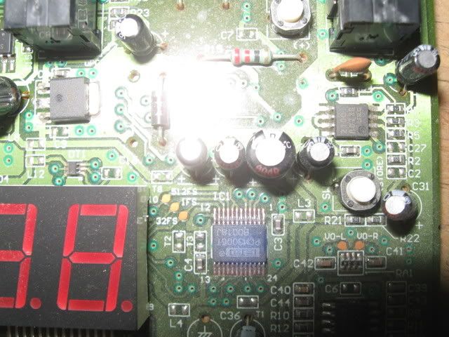
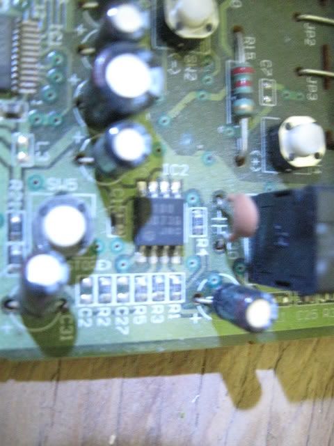
IC2 is a 2100 JRC, you can't tell in the picture since I suck at the photography. I couldn't find any information on it online.
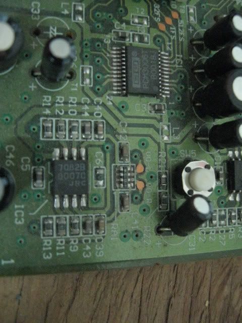
IC3 is another JRC chip, this time a 7082B low voltage CMOS power amp
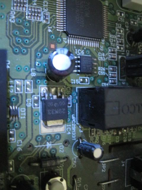
IC4 is a 29M33 voltage regulator
IC 5 is....IC5 is really freakin' small! It's a 4 pin SMD type package, and I can't make out any markings on it.
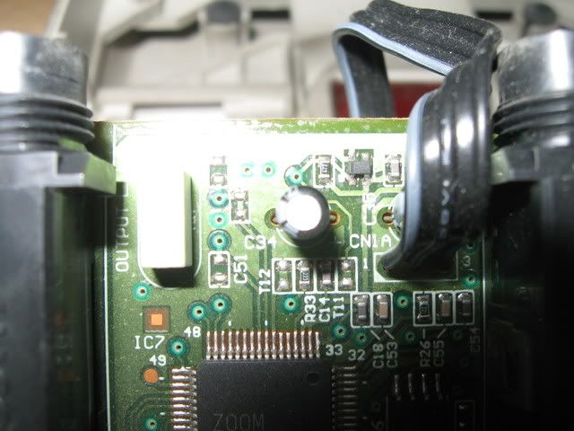
IC6 has the markings S93C5 6V02, which turns out to be a 2kb EEPROM. This is where all the custom settings are stored.
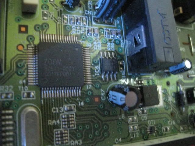
IC7 Ahh, now we get to the brains of the 505 II, at least one of them. This is one of their inhouse chips, with the markings ZOOM 505II 0001, which I'm guessing the 0001 is a revision number. I've only taken this one apart, so I don't know if there were any other chips in the series. 0017KP007 is also printed below the previous markings.
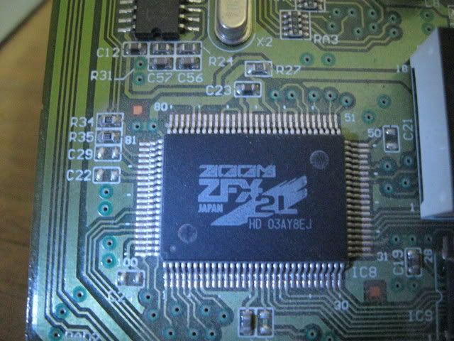
IC8 The other half of the brains, the ZFX2L chip, also made inhouse by Zoom.
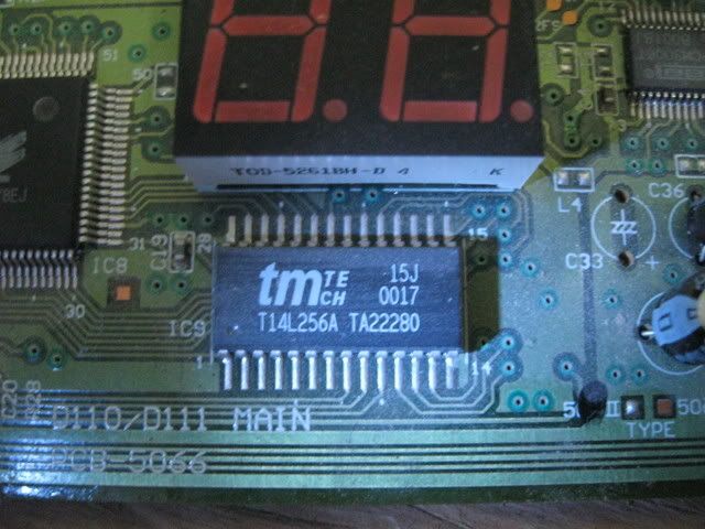
IC9 is a fairly large chip, with the markings T14L256A TA22280. This one turns out to be a high speed CMOS static RAM chip.
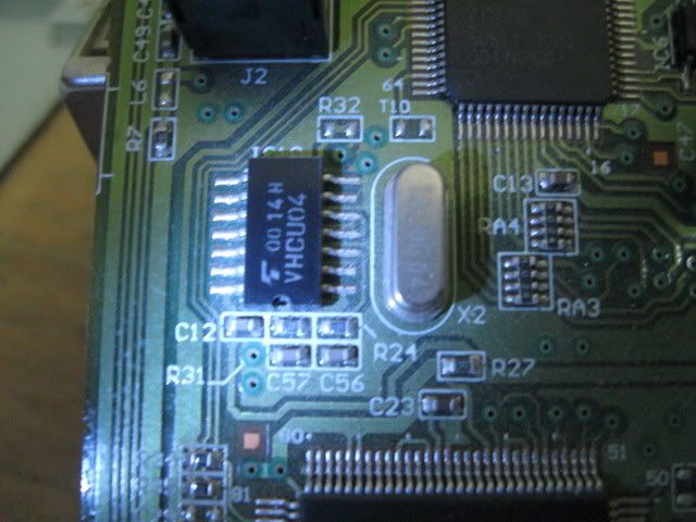
And finally, the last one, IC10. IC10 is stamped with VHCU04, and it seems to be a hex inverter. What it's used for, your guess is as good as mine, but I think it might form some sort of bridge between the 505 II chip and the ZFX2L.
Now on to the board itself. A good deal of the components are SMD, though there are quite a few thru-hole caps, and one resistor. Also, the LED display is thru-hole, which is very important for the second part of this article, which will be published at a much later date, once I return to the states.
Some other things, as I was looking over the board, I noticed about 10 or so "test points", little gold pads at various places on the board. Some of them are labeled, VO-L and VO-R, which I think is an output test point, 512FS, 1FS, and 32FS. Not sure what these are for. The only other one that I can make any sense of is on pin 50 of the 505 II chip.
Near the bottom of the board it gets real interesting. There are two test pads, not included in the 10 I mentioned above, with one of them having a blob of solder covering it. They are labeled 505 II and 506 II. The Zoom 506 II is a bass effects processor. The question that comes to mind, is how different are the 505 II and the 506 II? There's a couple of empty places on the board, for various SMD capacitors, and there's one thru hole empty spot for a RF choke(I think) and a diode. I'll try and get my hands on a 506 II and see what the difference is. The 506 II seems to be a bit rarer than the 505 II, at least in my experience. If anyone has one they want to donate, or even just open up and take a few pictures, send me an email!
Well, that's about it for the Zoom 505 II tear down. If I ever get my hands on another one of these little buggers, I plan on playing around with it a bit more, maybe changing out the silicon diode for another one, and adding one in the open spot. As always, I hope you enjoyed the article as much as I did writing it. Any questions, comments or complaints can go to my email joshhoose@gmail.com or posted here as a comment.